Something to look forward to: Intel submitted several research papers to this year’s International Electron Devices Meeting (IEDM), highlighting their plans to pursue new 2D transistor materials and 3D packaging solutions. The new information backs CEO Pat Gelsinger’s previous statements regarding Intel’s upcoming microarchitecture design innovations. According to Intel’s Gary Patton, the new advancements will keep Moore’s Law alive and well for the foreseeable future.
Earlier this year, Nvidia’s Jensen Huang declared Moore’s Law dead (again) during a 4000-series launch Q&A session. The prediction echoed similar statements made by Huang during the 2017 Beijing GPU Technology Conference. And much like those times before, Intel isn’t buying what Nvidia’s leather leader is selling.
The company’s 2023 IEDM research submissions highlight several processes, materials, and technologies that could help the semiconductor giant to support their previous statements on delivering chiplet-based trillion transistor processors by 2030.
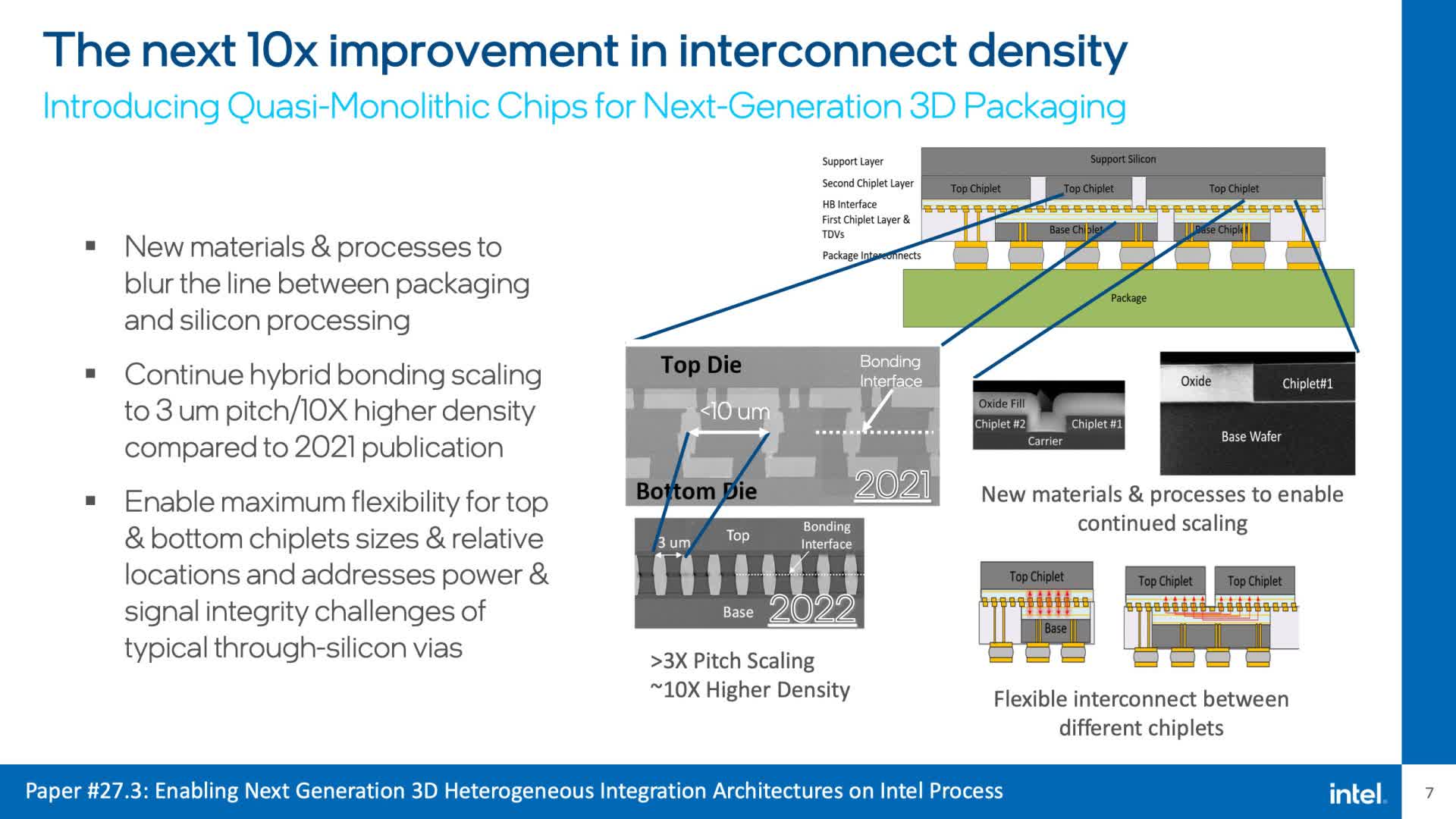
Intel’s new transistor and packaging research is primarily focused on advancing CPU performance and efficiency, closing the distance between traditional single-die processors and new chiplet-based designs. Some of the concepts presented in the submitted materials include greatly reducing gaps between chiplets to improve performance, transistors capable of retaining their state even after losing power, and new stackable memory solutions.

Gary Patton, Intel’s vice president and general manager of Components Research (CR) and Design Enablement, said that “seventy-five years since the invention of the transistor, innovation driving Moore’s Law continues to address the world’s exponentially increasing demand for computing. At IEDM 2022, Intel is showcasing both the forward-thinking and concrete research advancements needed to break through current and future barriers, deliver to this insatiable demand, and keep Moore’s Law alive and well for years to come.”
The CR group’s research has identified new processes and materials critical to driving the company closer to their trillion-transistor milestone. The company’s latest hybrid bonding research shows a 10x improvement over the previous year’s presentation. Other research showcased by Intel’s submissions includes designs using novel materials with thicknesses not exceeding three atoms, memory that can be placed vertically above transistors, and a greater understanding of interface defects that can negatively impact quantum data storage and retrieval.

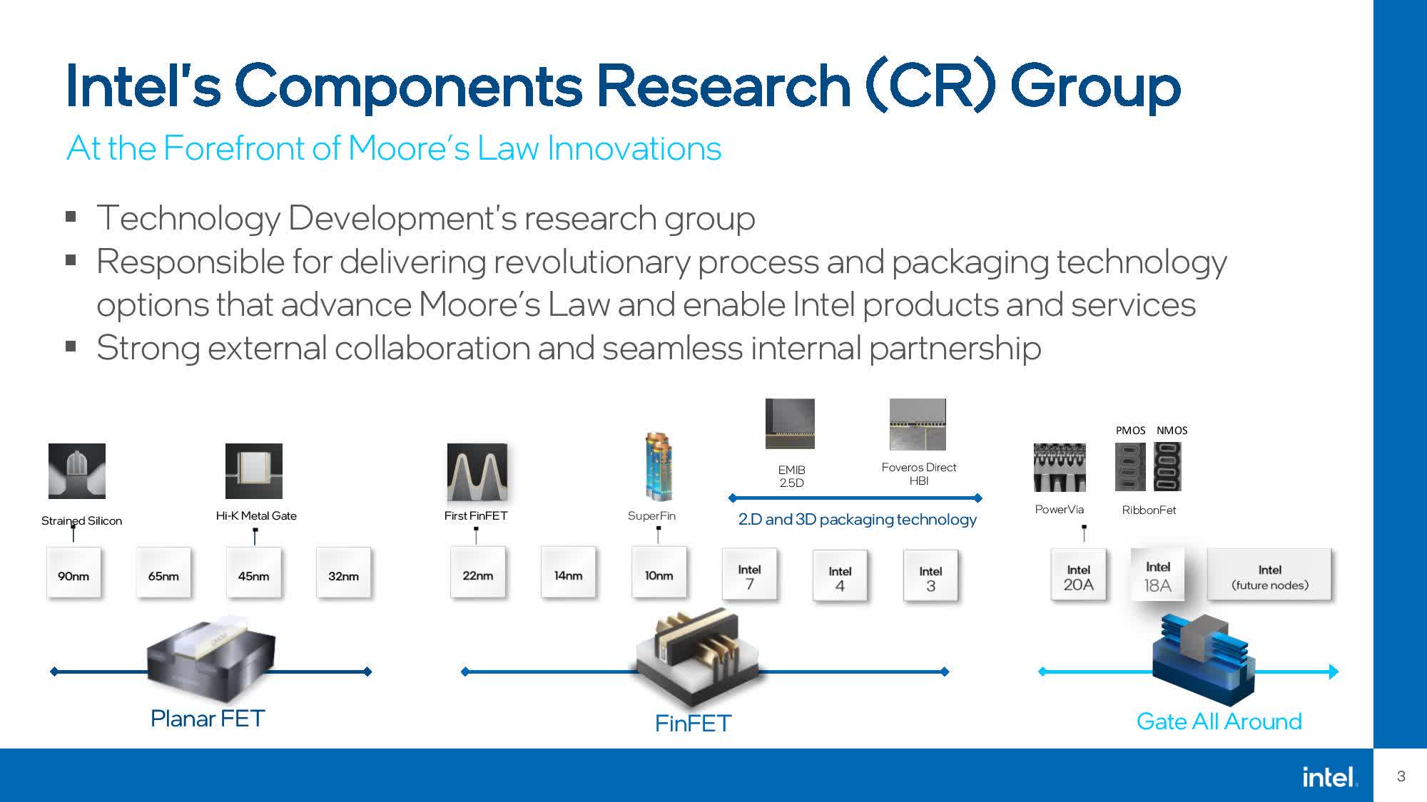
Intel’s Components Research Group serves as the company’s internal leader for new and groundbreaking technology development. CR engineers invent and develop new materials and methods that support semiconductor manufacturers in the ongoing battle to shrink technology to the atomic scale. The group is responsible for Intel’s extreme ultraviolet lithography (EUV) technology, which has been integral to its ability to continue shrinking node sizes while increasing overall semiconductor capabilities. The group’s work and timelines are typically five to 10 years ahead of commercially available technologies.


